Embedded Modules
Seven embedded modules provide autonomous capabilities to the self-driving vehicle. * TODO: * Assign each module an ID and describe them here

SDV Modules, Sensors and Computing Devices
CAN Communication
Install NVIDIA SDK Manager
Download and run SDK Manager on your host machine.

SDK Manager from NVIDIA
https://docs.nvidia.com/drive/archive/5.1.0.2L/sdkm/download-run-sdkm/index.html
Launch SDK Manager from terminal, using the parameters below to run an installation from the command line. In our case we used the sdk manager from cli for the Jetson Xavier AGX
Example:
./sdkmanager --cli install --user john.doe@example.com --logintype devzone --product Jetson --version 5.2 --targetos Linux --host --target P2888 --flash all
https://docs.nvidia.com/sdk-manager/sdkm-command-line-install/index.html
After downloding Linux for tegra, use source_sync.sh script to sync kernel and u-boot source code.
Enter to Linux_for_Tegra/bootloader/t186ref/
Decompile dtb to dts for editing:
dtc -I dtb -O dts -o tegra194-a02-bpmp-p2888-a04.dts tegra194-a02-bpmp-p2888-a04.dtb
Change the clock to PLLC or PLLAON, the correct register is in Linux_for_Tegra/source/public/hardware/nvidia/soc/t19x/kernel-include/dt-bindings/clock/tegra194-clock.h In our case, the options were:
#define TEGRA194_CLK_CLK_32K 289U //0x121, 32K input clock provided by PMIC
#define TEGRA194_CLK_OSC 91U //0x5b, input from Tegra's XTAL_IN
#define TEGRA194_CLK_PLLC 314U //0x13a, PLL controlled by CLK_RST_CONTROLLER_PLLC_BASE
#define TEGRA194_CLK_PLLAON 94U //0x5e, PLL controlled by CLK_RST_CONTROLLER_PLLAON_BASE for use by IP blocks in the AON domain
We used the PPLC so in the dts file, we modified it to:
clock@can1 {

     allow_fractional_divider = <0x01>;
     allowed-parents = <0x121 0x5b 0x13a 0x5e>;
     clk-id = <0x09>;
};
clock@can2 {

     allow_fractional_divider = <0x01>;
     allowed-parents = <0x121 0x5b 0x13a 0x5e>;
     clk-id = <0x0b>;
};
8. Compile back dts to dtb:
dtc -I dts -O dtb -o tegra194-a02-bpmp-p2888-a04.dtb tegra194-a02-bpmp-p2888-a04.dts
Finally, you need to display * The [bpmp-fw-dtb] has been updated successfully. *
Enter to Linux_for_Tegra
Copy the .cfg to the bootloader that we previously installed with the source_sync.sh:
cp bootloader/t186ref/BCT/tegra194-mb1-bct-ratchet-p2888-0000-p2822-0000.cfg bootloader
Whether it is in Linux_for_Tegra folder or inside the jetson after flashing the device, You have to change the device tree node mttcan@c310000, mttcan@c320000 and attached pllaon or pplc and The clock.
Enter to Linux_for_Tegra/source/public/hardware/nvidia/platform/t19x/galen/kernel-dts/common/tegra194-p2888-0001-p2822-0000-common.dtsi
Modify the clock-init
clocks-init {

             compatible = "nvidia,clocks-config";
             status = "okay";
             disable {

                     // clocks = <&aon_clks TEGRA194_CLK_PLLAON>,
                     //   <&bpmp_clks TEGRA194_CLK_CAN1>,
                     //   <&bpmp_clks TEGRA194_CLK_CAN2>;
             };
     };
Enter to Linux_for_Tegra/source/public/hardware/nvidia/platform/t19x/galen/kernel-dts/common/tegra194-p2888-0001-p2822-0000-common.dtsi
16. Modify the device tree for pplaon or pplc ::
mttcan@c310000 {

   status = "okay";
   pll_source = "pllaon";
   clocks = <&bpmp_clks TEGRA194_CLK_CAN1_CORE>,
      <&bpmp_clks TEGRA194_CLK_CAN1_HOST>,
      <&bpmp_clks TEGRA194_CLK_CAN1>,
      <&bpmp_clks TEGRA194_CLK_PLLAON>;
   clock-names = "can_core", "can_host","can","pllaon";
};

mttcan@c320000 {

   status = "okay";
   pll_source = "pllaon";
   clocks = <&bpmp_clks TEGRA194_CLK_CAN2_CORE>,
      <&bpmp_clks TEGRA194_CLK_CAN2_HOST>,
      <&bpmp_clks TEGRA194_CLK_CAN2>,
      <&bpmp_clks TEGRA194_CLK_PLLAON>;
   clock-names = "can_core", "can_host","can","pllaon";
};
17. Inside the Linux_for_tegra that has the bootloader, use the flash.sh. In our case it was the Jetson-Xavier AGX:
sudo ./flash.sh -k bpmp-fw-dtb jetson-agx-xavier-devkit mmcblk0p1
For more information about how to flash your board, read the /txt posted in the forum: https://forums.developer.nvidia.com/t/jetson-xavier-agx-error-flash-sh/174572/6
19. Check CAN Is your master clock pll_aon, If it is pll_c or osc. If it is osc , it was not successful your tests.
sudo cat /sys/kernel/debug/bpmp/debug/clk/can1/parent
pll_aon
If the clock is changed to pllc or pll_aon continue to step 24 or check https://forums.developer.nvidia.com/t/how-to-use-vector-can-analyzer-in-jetson-tx2/63300/2.
Insert CAN BUS subsystem support module.
modprobe can
Insert Raw CAN protocol module (CAN-ID filtering)
modprobe can_raw
23. Real CAN interface support (for our case, it is: mttcan)
modprobe mttcan (dependent module is can_dev: can driver with netlink support)
Disable can0 or can1 to change bitrate.
sudo ifconfig can0 down
CAN interface settings for both the controllers, change the bitrate depending on the can device you are using.
ip link set can0 type can bitrate 500000 dbitrate 2000000 berr-reporting on fd on
ip link set up can0

ip link set can1 type can bitrate 500000 dbitrate 2000000 berr-reporting on fd on
ip link set up can1
CAN interfaces are up now. Use ifconfig to list all the interfaces which are up. Installation of user app to check CAN communication
sudo apt-get install can-utils
Commands to run to check CAN packet send/receive. Broadcasting a can data packet:
cansend <can_interface> <can_frame>
e.g. cansend can0 123#abcdabcd
Receiving a can data packet:
candump can_interface
e.g. candump can1
Different tools (i.e. cangen, cangw etc) can be used for various filtering options. To check the interface statistics
ip -details -statistics link show can0
ip -details -statistics link show can1
29. To read info from the Can Bus use candump.
candump -ta -x can0
Important Info: To manually download and expand the kernel sources, in a browser, navigate to https://developer.nvidia.com/embedded/downloads, to locate and download the L4T source files for your release.
CAN STM32
The following table displays the CAN frame we use to interact with the Jetson-Xavier and SMT32 modules, including the header, data, and description to assist programmers understand the car’s functions.
JETSON Xavier TX Messages
Module
Jetson ID-TX
Data
Description
Panel
333
16
Inferior Left Front - Turn Off
Panel
333
15
Inferior Right Front - Turn Off
Panel
333
14
Upper Left Front - Turn Off
Panel
333
13
Upper Right Front - Turn Off
Panel
333
12
Horn - Turn Off
Panel
333
11
Wiper - Turn Off
Panel
333
6
Inferior Left Front - Turn On
Panel
333
5
Inferior Right Front - Turn On
Panel
333
4
Upper Left Front - Turn On
Panel
333
3
Upper Right Front - Turn On
Panel
333
2
Horn - Turn On
Panel
333
1
Wiper - Turn On
Throttle
334
X
Wiper position change, data=Velocity steps
Throttle
335
X
Set Max Speed, data=Max speed
Steering wheel
338
X
Set Steps, data=steps
Steering wheel
339
1
Change of direction, right
Steering wheel
339
2
Change of direction, left
Steering wheel
340
1
Enable driver
Brake
341
X
Set Steps, data=steps
Brake
342
1
Change of direction, right
Brake
342
2
Change of direction, left
Brake
343
1
Enable driver
Transmission
344
X
Set Steps, data=steps
Transmission
345
1
Change of direction, right
Transmission
345
2
Change of direction, left
Transmission
346
1
Enable driver
STM32 TX Messages
Module
STM32 ID-TX
Data
Description
Panel
222
1
Success
Panel
222
2
Error
Throttle
222
1
Success
Throttle
222
2
Error
Brake
222
1
Success
Brake
222
2
Error
Transmission
222
1
Success
Transmission
222
2
Error
The CAN Rx Task analyzes CAN frames to activate flags and variables.

The CAN Header analysis function is shown below.

The CAN Tx Task transmits success or error signals based on previous implementations.


The Task Panel toggles GPIO based on CAN message data.

The TaskPot can modulate a digital potentiometer to regulate automobile velocity and set its maximum value depending on CAN message data.


Common Module Subsystems
SDV modules are similar (with slight variations) in certain subsystems, such as in IO, and power supply.
STM32
The STM32L431RCT6 <https://www.st.com/en/microcontrollers-microprocessors/stm32l431rc.html is chosen as the main microcontroller unit for all modules to follow an standard started by the development of the USV and UUV PCBs, where a similiar version was used, which in turn eases the electronics and embedded development.

STM32 Base Configuration
High-Speed External Clock
The oscillator design guide for mcus <https://www.st.com/resource/en/application_note/an2867-oscillator-design-guide-for-stm8afals-stm32-mcus-and-mpus-stmicroelectronics.pdf> was used to select the oscillator circuit components.
The high-speed external clock is supplied with a 16MHz as the crystal oscillator.
The selected crystal <https://www.lcsc.com/product-detail/Crystals_Yangxing-Tech-X322516MLB4SI_C13738.html> has a load capacitance (CL) of 9pF and, assuming a stray PCB capacitance (Cs) of 3pF, two 12pF capacitors (CL1, CL2) were chosen following the next equation.

Crystal Load Equation

Oscillator Circuit
STM32 Programming, Supply and Communications
An ST-Link is used to program the STM32 via a 10 pin header 1.27mm pitch.
A 5-pin M12 connector is used to supply +12V, and to connect the module to the CAN Bus. The 5th pin is left unused.

Programming, Supply and Comms
An ST-Link is used to program the STM32 via a 10 pin 1.27mm-pitch header.
A 5-pin M12 connector is used to supply +12V and to connect the module to the CAN Bus. The 4th pin is left unused, connected to GND.

M12 Connector Pinout
CAN
The TCAN330GD <https://www.ti.com/lit/ds/symlink/tcan332g.pdf?HQS=dis-mous-null-mousermode-dsf-pf-null-wwe&ts=1665117642045&ref_url=https%253A%252F%252Fwww.mouser.mx%252F> is the CAN transceiver used to provide an interface to the CAN bus.

CAN Transceiver Circuit
Module ID
Each module can be mannually assigned an ID, which can be used for the CAN messages identification. A maximum of 16 IDs can be assigned.

Module ID selection
Power Supply

Base power supply configuration
- The power supply subsystem provides power to the whole module which we plan to use 12V, it contains:
A 1A fuse for overcurrent protection.
Reverse polarity voltage protection
12V to 3.3V DC Converter
12V to 5V DC Converter (optional)
LEDs as power indicators
NTC thermistor for the regulators temperature
Reverse Polarity Protection
For reverse polarity voltage protection with mosfets, a couple of things should be considered.
The mosfet drain-source current (Ids) must withstand the module current requirements.
- The drain-source voltage (Vds) must be larger than BATT+.
A NDS352AP <https://www.mouser.mx/ProductDetail/onsemi-Fairchild/NDS352AP?qs=mdiO5HdF0KhbUArAR6yyEg%3D%3D> mosfet is chosen, with a Vds = 30V and the maximum value of Drain Current (ID) of -1.3 A.
- The gate-source voltage (Vgs) must not be surpassed by BATT+. A zener must be added to protect the mosfet in the case that BATT+ is larger than Vgs.
The NDS352AP Vgs = 20V, so a MMSZ4702T1G https://www.lcsc.com/product-detail/Zener-Diodes_onsemi-MMSZ4702T1G_C242274.html zener with a Zener voltage of 15V is chosen.
The drain-source resistance (Rds) must be as low as possible, for low power dissipation.
Unlike using a diode, this circuit does not step down the voltage as a mosfet is being used to open or close the circuit.
The LTSpice simulation showcases the correct operation of the circuit.

Base Reverse Polarity Voltage Protection Circuit
DC Converters
Depending on the module, a single 12V to 3.3V plus a 12V to 5V could be used, both with a maximum output current of 1A. The regulators employed are:
R-785.0-1.0 <https://www.mouser.mx/ProductDetail/RECOM-Power/R-785.0-1.0?qs=YWgezujkI1LK5NzKL%2Fc9sg%3D%3D>
R-783.3-1.0 <https://www.mouser.mx/ProductDetail/RECOM-Power/R-783.3-1.0?qs=XF8hdbuHJAVK%252BT0VfuIcYQ%3D%3D>
I/O
IO for all modules is usually based on the use of an optocoupler to isolate inputs from the module circuits.
As input voltages may range from 5V to 12V (or more), a constant current (~15mA) circuit is required to power the optocoupler LED. More on this here <https://www.instructables.com/Circuits-for-using-High-Power-LED-s/> and here <https://www.ti.com/lit/wp/slyy163/slyy163.pdf?ts=1664295229681&ref_url=https%253A%252F%252Fwww.google.com%252F>.
The transistors used are BC817-40,215 <https://www.lcsc.com/product-detail/Bipolar-Transistors-span-style-background-color-ff0-BJT-span_Nexperia-BC817-40-215_C52801.html>, which withstand a maximum collector-emiter voltage of 45V.

IO Base Configuration
Stepper-Based Modules
The steering and pedal brake modules share essentially the same purpose: control stepper motors and read encoder and brake signals (optional). For this reason, the PCB for both modules is exactly the same.
I/O
The brake module reads a signal proceeding from the pedal brake that indicates that the pedal is being pressed.
The steering module does not required external inputs.
Encoder
The steering module considers an absolute encoder to provide feedback on the steering angle. The sensor used is the RM8004 <https://www.ifm.com/es/es/product/RM8004>. This encoder is connected directly to the CAN bus.

Encoder M12 Connector
Pin |
Meaning |
1 |
CAN_GND |
2 |
VBBc |
3 |
GND (PE) |
4 |
CAN_HIGH |
5 |
CAN_LOW |
Decoupling Capacitors
For every power supply, there should be a 0.1 uF capacitor and a bigger one. This should be placed as physically close as possible to the correspondent pwer supply. Check the datasheet for the proer layout. This capacitors operate at a maximum 16V.
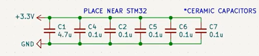
Capacitors array
Power supply for ADCs
This power supply makes use of a ferrite bed. More specifically it is use for thermistors.

ADCs supply
RJ45 Ethernet Connector

RJ45 Connector
- |The following table represents the pin configuration for the RJ45.
Pin
Meaning
1
CAN_HIGH
2
CAN_LOW
3,4,5
GND (PE)
6
Emergency button
7,8
BATT
9
CAN HEART BIT
10,12
GND
11
Emergency button LED
Comms submodule
For the CAN communication with the module two different tranceivers can be used; TCAM330G or MAX33040EAKA. As of now the TCAM330 serves as the main tranceiver and the MAX330 is a substitute if needed. The image and pinout below shows the MAX330.
Pin
Meaning
1
CAN_TX1
2
GND
3
VDD(DecouplingCapacitor)
4
CAN_RX1
5
SHDN - turn off chip
6
CAN_LOW
7
CAN_HIGH
8
STBY - CHIP HOLD
It is worth mentioning that PIN 6 and 7 (CAN HIGH and CAN LOW) are connected to a TUBC doide for “electrostatic discharges” protection.

MAX33040EAKA Tranceiver
For either of this tranceivers there are resistors that help with the connection with the STM32, the RJ45 and the support JSTs.

Tranceiver resistors
CAN topology The CAN topology implemented in this project is “Daisy Chain”, which has the following structure.

CAN Topology
Encoders .. figure:: /images/electronics_embedded/stepper_steering_module/Encoders2.png
- align:
center
- alt:
stm32 schematic
- figclass:
align-center
- width:
600px
Encoders
DEBUGGING
The debugging components are quite simple. LEDs are installed with the purpose of knowing the value of different signals.
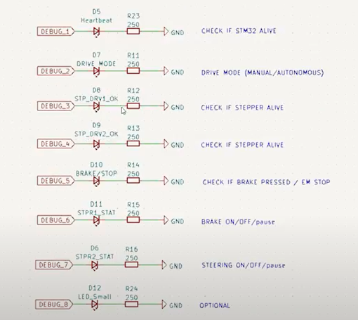
Debugging LEDs
A FTDI chip is used to connect via serial communication with the stm and read several values in a terminal.
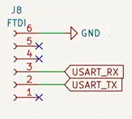
FTDI chip
Stepper Driver Connection
The main driver used for this module is the STP-DRV-6575

STP-DRV-6575
The following diagram shows the connections to the driver and its correspondent signals.

Connections layout
Here is an explanation if the driver’s input and output signals:
Signal
Meaning
STEP
given an impulse (010), moves 1 step
DIR
Clockwise/counterclockwise
EN
activate (0), deactivate (1)
Fault
Output for proper functioning
For more information about the input and output signals for the driver, it may be to refer to the official manual and data sheet.

Driver manual
The stepper motor used in the steering module is one of the stp-MTRH-42 variety (low voltage, higher torque). If a change is planned, it is important to change the compatibility table between the driver and steppers.
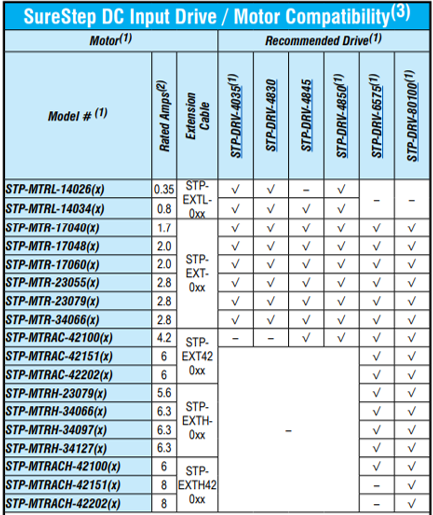
Compatibility table
Since the STM32 works with 3.3V and the driver works starting from 5V, a level shifter is implemented. This level shifter is the TXU0304PWR. ESD diodes are also implemented for static discharges protection.
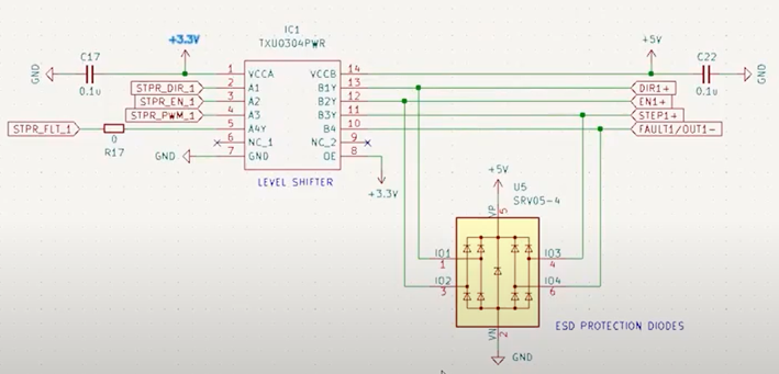
Level-shifter
Transmission Module
To be determined.
Throttle Module
This circuit can activate a relay module that is connected to the motor (Highlighted in orange). It is a switch that can turn on the motor. This module can also enable manual o automatic regulation of velocity with a digital potentiometer of 10k.

Motor Relay

General Diagram Throttle module with selected motor relay
Octocoupler SFH617A-1
CTR is defined as the ratio of the collector to the forward current expressed in percent. The collector current (Ic) is the current in the photo transistor while forward current is the current in the diode (If).
Signal
KiCad schematic
Vdd
Second
Vout
RelayMotor
Rf
VGS_sat (Mosfet).
Re
R6
IF
R7
Vf
Forward Voltage =1.35. According to datasheet
If
VGS_sat (Mosfet).
VCEO
VGS_sat (Mosfet).
CTR
60%

CTR configuration
Mosfet WST2N7002A
Vgs(th) max = 3 ( We are saturating it with 11.7V)

Mosfet GS(th) voltage
Vgs and Vds are not surpassing the maximum values.
.png)
Mosfet Graph (Vds/Id)
Vgs and Vds are not surpassing the maximum values.


Octocoupler maximum and minimum values VCE

LTspice Tests
We tested these equations with octocoupler PC817C and Mosfet QS6K1.

Ltspice diagram octocoupler and mosfet


LTspice test


Mosfet QS6K1 gate threshold voltage minimum and maximum values


LTspice test

Octocoupler collector-emitter saturation voltage minimum and maximum values.
Real-life Tests
Tests were made with mosfet and an arduino, we used a 1k pull down resistor. Link of video below.

Real life tests with mosfet

Kicad tests with mosfet
Curtis speed controller
Curtis speed controller is a device used for high precission motor speed control applications in electric vehicles. This controller modulates speed based on the low current entries J1, J2 and J3.

Curtis speed controller pins
Pins
Description
J1
Keyswitch, not used in this module
J2
Wire 1 of 2-wire throttle. Must be connected to Potentiometer High or ITS Throttle terminal.
J3
Wire 2 of 2-wire throttle. Must be connected to Potentiometer wiper, ITS Low terminal.
Digital Potentiometer
This circuit can enable manual o automatic regulation of velocity with a digital potentiometer of 10k. We are powering the potentiometer with 12 Volts, to modulate velocity we used the inputs A,B,W , in the terminal A or B will be entering 10V and the result will be going to the Wiper W and eventually will go to J3 from curtis controller.
DS3502U+
This was the original potentiometer used for autonomous mode control. However, this is not the main one anymore. Although the main potentiometer is MCP45HVX1, the circuit and logic behind works basically the same way.
Pin description of DS3502U+ potentiometer:

DS3502U+ potentiometer pin description
Pins
MCU /Car
RH
J2E / GND / -
RL
J2E / GND / -
V+
12V
SCL
SCL
A0
GND
A1
GND
VCC
3.3 V
SDA
SDA
DS3502U+ Potentiometer datasheet:

DDS3502U+ potentiometer maximum ratings
MCP45HVX1
It is the main digital potentiometer of the Throttle module. It works almost the same way than the DS3502U, but it includes some extra pins and another feautres.
This potentiometer also comunicates with the STM32 via I2C to modify or read the registers.
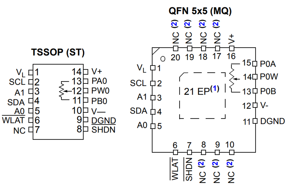
MCP45HVX1 potentiometer pin view
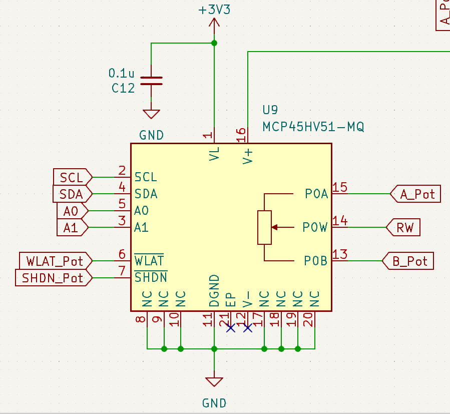
MCP45HVX1 circuit view
Pin description of MCP45HVX1:

MCP45HVX1 potentiometer pin view
Programming the MCP45HVX1
The development of the functions related to the control of this device is performed inside mcp45hvx1.c inside the throttle module STM32 project.

mcp45HVX1.c device initialization
At first, there is the definition of I2C address of potentiometer (pot_address), the TCON register (Terminal Control) that consists of 4 bits, and allows the developer which terminals (PA0, PW0, PB0) are going to be enabled and used for the circuit. Also, it is defined the enable_potentiometer and finally the name of the I2C handler (hi2c1) configured in the project.
In initialize_devices it determines if the connection with the potentiometer has been established. If this is performed successfully, then the potentiometer is enabled.

mcp45HVX1.c begin potentiometer function
begin_pot is the function where the initialization is completed. If the potentiometer is enabled, it starts setting the wiper register with the initial value with the direction 0b00
Then, the pin WLAT (wiper latch) is setted to LOW. As shown in the pin description, this allows the direct update of the wiper value. When it is HIGH, the new value received by the I2C message is first stored in the shift register. This feature allows the user to connect the wiper update using external events. For this implementation, this pin is only set once on LOW and used as a reset.
After that, the SHDN pin is set to HIGH. Its functionality is basically to be an enable for the potentiometer terminals.
Finally, it is called defaultTCON that configures the Terminal Control register.

mcp45HVX1.c write wiper function
The writeWiper function is used to update the value of the wiper calling write_register function on the 00 address.

mcp45HVX1.c write register and send command functions
Two of the most important functios are send_command and write_register.
write_register is in charge of write the register of a given address calling send_command with the command parameter of 0b00 which is used to indicate a writing operation.
send_command receive and address, a command which is a int, the data to be sent and the data size. Basically, this function executes all the logic needed to create the I2C message that will be sent to the potentiometer.
The writeWiper function is used to update the value of the wiper calling write_register function on the 00 address.

mcp45HVX1.c default terminal control register initialization
As mentioned before, the defaultTCON function is used to set the bits of the TCON register, and calls the function that writes it as write_wiper function does. This register is not being modified because the right terminal is directly conected to the relay circuit using a solder jumper.
Digital potentiometer pin description.
Pins
Meaning
Pot
Connected to GPIO of STM32 to switch motor.
J2E
This signal is connected to Curtis controller J2 , it has 10 Volts. When is manual mode,
it’s connected to WiperPot, and to Digital pot terminals in autonomous mode
WiperPot
Used for manual control, this signal corresponds to the HIGH terminal of manual pedal
potentiometer acoording to Curtis controller documentation.
J3
The modulated signal will come from the wiper (W) and be connected straight to J3
CurtisController. This is also connected to the wiper terminal of the manual pedal

Digital Potentiometer schematic

Throttle module in general diagram
Why A0 and A1 is connected to GND?
The DS3502’s slave address is determined by the state of the A0 and A1 address pins. These pins allow up to four devices to reside on the same I2C bus. Address pins tied to GND result in a 0 in the corresponding bit position in the slave address. Conversely, address pins tied to V CC result in a 1 in the corresponding bit positions. For example, the DS3502’s slave address byte is 50h when A0 and A1 pins are grounded. I 2 C communication is described in detail in the I 2 C Serial Interface Description section.

DS3502 Slave Address Byte
Why VDD has decoupling capacitors?
To assist smooth out any low-frequency variations in an input voltage, a 10uF capacitor is placed farthest from the IC. Then comes the 0.1uF capacitor that is located the closest to the IC. This one will assist in eliminating any high-frequency noise in your circuit. You can provide your IC a constant, smooth voltage to operate with by connecting these two capacitors together. Things to consider in layout with decoupling capacitors:
Placement: Whether your power supply is 3.3V or 5V, you should always connect your decoupling capacitors to ground.
Distance: Decoupling capacitors should always be positioned as close as feasible to your integrated circuit. They will be less effective the further away they are.
Ratings: For each integrated circuit on your board, It is generally advised adding a smaller 0.1-10uF electrolytic capacitor and a single 100nF ceramic capacitor.

Digital Potentiometer power supply with decoupling capacitors
Why so many 0 resistors in Terminal A and B?
A zero-ohm link or zero-ohm resistor is a wire link packaged in the same physical package format as a resistor. Wiring alternatives for the experiments we conducted included connecting J2 of the Curtis controller to A and receiving the modulated voltage in W at J3 of the Curtis controller. Likewise, by connecting J2 in the other direction to B and giving W the modulated voltage. In the first experiment, we increase one vehicle’s speed from 2 to 5 km/h while decreasing the other from 24 to 36 km/h. Personally, I think J2 ought to be linked to B, J3 ought to be connected to W, and A shouldn’t be connected to ground. There will always be a chance for a modification with the 0 resistors, though, if I am mistaken.

Digital Potentiometer schematic showing RH,RW,RL
Tests with Digital Pot X9c103s 10k and Pot5k
We carried out a number of experiments and found that the speed could be modulated, going from 35 to 24 km/h. If we switched the terminals A and B to GND and VCC, we saw that the speed increased to 2 to 4/5 km/h. We assumed that the reason for the slight fluctuation was that we are utilizing a voltage divider in J2 from Curtis Controller. It would occur in the throttle pedal since it doesn’t require the voltage divider. However, X9x1903s can only accept a maximum voltage of 5 volts; in our previous experiments, we entered 3 volts into the chip. Other thing that we noticed is that because of the voltage divider J2 was always connected to Ground , that is why we couldn’t achieve a proper modulation of velocity.

Arduino Graph with ADC input and digital control
Tests were made with a 10k potentiometer to see if J2 and J3 can modulate velocity in Curtis controller, it worked exactly as the 5k pedal in our car.

Manual test with 5k potentiometer
Throttle module STM32 Programming
On this section we will describe the most important pieces of the code running on the STM32 inside the Throttle module.
Pin definition

STM32 Throttle module pin definition.
Pin description:
Pins |
Name |
Description |
PA6 |
WLAT |
Wiper Latch of the potentiometer. Used as a reset. Set during initialization |
PA7 |
SHDN |
Shutdown pin of potentiometer. Used as enable. Set during initialization |
PA9 |
Pot |
Pin used for changing the input of the Curtis Speed Controller: manual mode with 5k pedal or autonomous mode with digital potentiometer |
PA10 |
RelayMotor |
Pin used to change the state of the motor relay (see more) |
PA11 |
CAN1_RX |
Pin assigned to CAN RX channel |
PA12 |
CAN1_TX |
Pin assigned to CAN TX channel |
PB6 |
I2C1_SCL |
Clock of I2C interface for the digital potentiometer |
PB7 |
I2C1_SDA |
Data channel of I2C interface for the digital potentiometer |
PA3 |
hand_brake |
Input pin for the hand_brake signal |
main.c
The main file is in charge of calling all the initialization of ports, devices, interfaces and tasks to be excecuted.
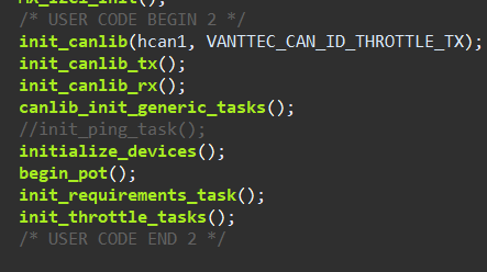
main.c initialization
It starts with the initializaton of canlib with ID VANTTEC_CAN_ID_THROTTLE_TX to declare the message transceiver id, after that, it initializes the functionality of transmission and reception of CAN messages, and the basic tasks of receive, send, reed and hanlde the message queue.
As show before, initialize_devices and begin_pot do the initial setup for the digital potentiometer.
Then, it initializes the proper tasks of the throttle as init_requirements_task where there are the functions that hanldes the basic requirement signals as emergency stop, reverse, etc.; manipulating the values of the RX messages. On the other hand, init_throttle_tasks there are tasks that update the values of the pins, read the hand brake input and control the digital potentiometer.
Throttle tasks
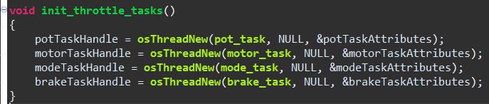
Throttle tasks initialization
This function creates all the threads for each task to perfom the control of Throttle module:
Manage and update the potentiometer.
Enable the motor.
Switch of drive mode.
Reading of hand brake input.
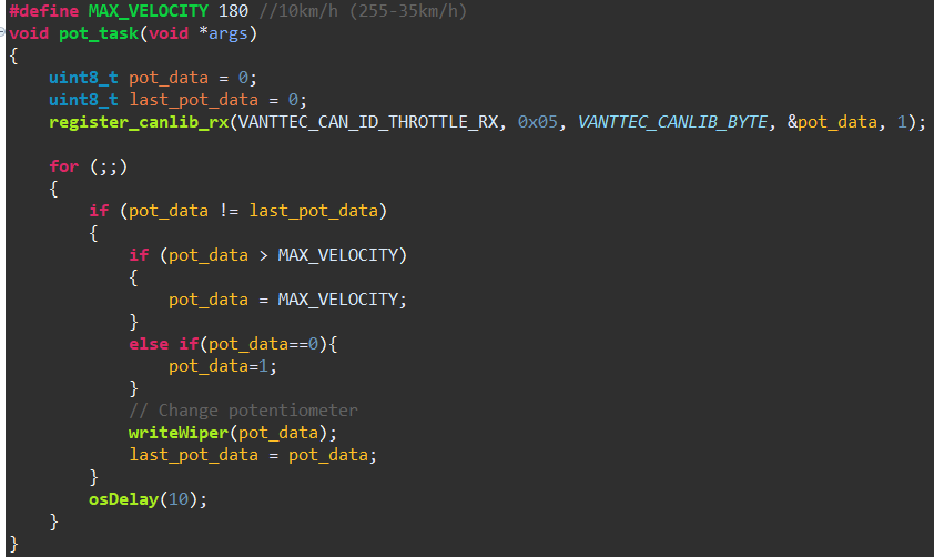
Potentiometer task
pot task is in charge of receive the messages of the CAN device id of VANTTEC_CAN_ID_THROTTLE_RX, and message id 0x05 (this is the one assigned to messages of digital pot value). The data is stored on pot_data variable.
In the excecution loop, it performs the logic to update the digital potentiometer. If it is a different value from the last one, checks if it is above the maximum permitted value, in case of true, then it sets the value to be the maximun. Also, it checks if it is 0, and then corrects it to 01. Finally, it updates the wiper calling writeWiper and updates the last data variable.

Motor enable task
In the motor_task, it will subscribe the messages of the CAN device id of VANTTEC_CAN_ID_THROTTLE_RX, and message id 0x06 (this is the one assigned to messages of motor signal). The data is stored on motor_data variable.
In the excecution loop the task will check if motor_data is 1, in this case it will write a HIGH on the RelayMotor pin to activate the relay. In any other case it will write a LOW and return the Relay to default.
When the relay is activated, the motor is energized directly (this is used for autonomous mode). If it is on default/common-closed state, the motor will only be powered when the driver press the manual pedal and activates the pedal swtich (this is used for manual mode).
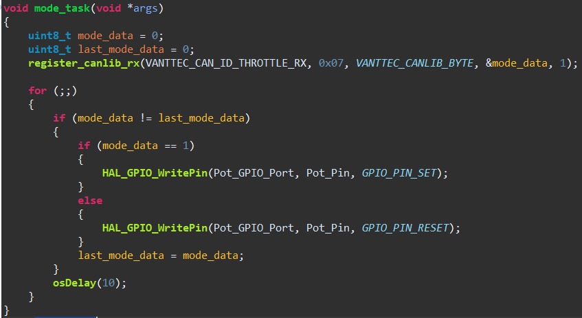
Drive mode task
The mode_task is very similar to the motor_task in terms of logic, becuase it subscribes a CAN message and based on that entry it decides when to set the output pin (Pot_pin). In this case, the tasks receives the messages from VANTTEC_CAN_ID_THROTTLE_RX, and message id 0x07 (this is the one assigned to messages of drive mode signal).
When mode data is 1 it means that autonomous mode is set and then writes HIGH in Pot and actives the potentiometer relay so J2E receives the value from the digital potentiometer terminals. In any other case, the pin is set to LOW and the relay will be on default/common-closed state so J2E switches to the high terminal of the pedal potentiometer (wiperPot on the circuit).

Hand brake input task
In brake_task, the function reads the status of the input pin of brake (hand_brake) to check if it has been activated.
If the brake status is different from previous one and the brake is activated (brake_status = 1), then, it sets the digital potentiometer value to 0 (which means setting speed to 0), it chages ti manual mode seding a 0 with the message id of 0x07 (drive mode message), and deactivate the motor relay sending a 0 with the message id of 0x06 (motor data message).
For any case, it sends the the updated brake data in can message. Remember that for transmission this module uses VANTTEC_CAN_ID_THROTTLE_TX and with message id of VANTTEC_CAN_ID_FRENO_MANUAL
NOTE: the action of sending the new values is done with update_table, a function in canlib module that given a devide id, and message id, update the values on the CAN message table, sending the new data.
Requirement tasks
This functions are inside ThrottleVantec/Core/Src/requirements.c

Requirements task initialization
This function creates all the threads for each tasks that covers the expected requirements of the car, such as:
Emergency stop.
Switch to autonomous/manual mode.
Reverse.
Hand brake activation.
Driver fault signal.
This functions are inside ThrottleVantec/Core/Src/requirements.c

Emergency stop task
In emergencystop_task the function susbscribes to the emergency stop signal messages from the device VANTTEC_CAN_ID_GENERAl_TX (basically the central unit) with message id of VANTTEC_CAN_ID_ESTOP.
If a 1 is received, then the emergency stop signal is activated so the function perfoms the logic to stop the car, similar to what was done on hand_brake task:
Set speed to 0, updating the value on the message id 0x05 (potentiometer value), set a LOW on the RelayMotor pin sending a 0 with the message id of 0x06, and toggle to manual mode sending a 0 with the message id 0x07. Remember all these value are sent with VANTTEC_CAN_ID_THROTTLE_RX device id
Finally, the function also updates the value of VANTTEC_CAN_ID_ESTOP meessage with a 0 to indicate that the action has been performed.

Drive mode requirement task
In drivemode_task the function susbscribes to the emergency stop signal messages from the device VANTTEC_CAN_ID_GENERAl_TX (basically the central unit) with message id of VANTTEC_CAN_ID_DRIVE_MODE. If a 1 is received then the autonomous mode is set, in case to be 0, it is set the manual mode.
For autonomous mode, the function sends a 1 with the message id of 0x07 (remember mode_task). Then updates the initial potentiometer value of 2 with the message id 0x05 (remember pot_task) and finally sends a 1 with the message id 0x06 to energize the accelerator directly.
In case that it receives a 0, then it set up the manual mode in a very similar way as the hand brake and emergency stop tasks *.
For any of these cases, the function updates the VANTTEC_CAN_ID_DRIVE_MODE message to acknowledge the action has been performed
*NOTE: remember that when motorRelay pin is set to LOW does not mean the accelerator does not receive current, but it is only energized when manual pedal swith is pressed.

Reverse mode requirement task
In drivemode_task the function susbscribes to the emergency stop signal messages from the device VANTTEC_CAN_ID_GENERAl_TX (basically the central unit) with message id of VANTTEC_CAN_ID_REVERSE.
If a 1 is received then the reverse is active and it will set potentiometer value to 0 and set manual mode the same way has been done on brake task, drivemode task, etc. This is because reverse is only handled manually.
When it has finished it updates the value of VANTTEC_CAN_ID_REVERSE message to 0 as an acknowledge.

Hand brake requirement task
In frenomanual_task no further actions are needed because all the logic related to hand brake handling it is being performed by brake_task inside the Throttle tasks.

Driver fault requirement task
In drivemode_task the function susbscribes to the emergency stop signal messages from the device VANTTEC_CAN_ID_STEPPER_TX with message id of VANTTEC_CAN_ID_DRIVER_FAULT.
The principles are the same as in emergencystop_task. The function checks if the received value is 1 (indicating that there is driver fault). In that case, it will excecute the same routine of setting potentiometer value to 0 and changing to manual mode that has been explained before.
Once it has finished, then updates the VANTTEC_CAN_ID_DRIVER_FAULT message with 0 as an acknowledge.
References
Link of tests in drive link: https://drive.google.com/drive/folders/1uXBLU69br4WVwCLYkIgSi3tL1Cs67hec?usp=sharing
Datasheet, LSCS or mouser link:
Mosfet WST2N7002A: https://www.lcsc.com/product-detail/MOSFETs_Winsok-Semicon-WST2N7002A_C2830888.html
PC817C: https://pdf1.alldatasheet.es/datasheet-pdf/view/43376/SHARP/PC817C.html
Mosfet QS6K1: https://www.mouser.com/datasheet/2/348/qs6k1-210565.pdf
STM32L432xx: https://datasheet.lcsc.com/lcsc/1811081824_STMicroelectronics-STM32L431CBT6_C277951.pdf
Link of various tests in drive link: https://drive.google.com/drive/folders/1PjMfXWRD-9Su_6FwQhY2J2OD5yJEoXE3?usp=sharing